

详情
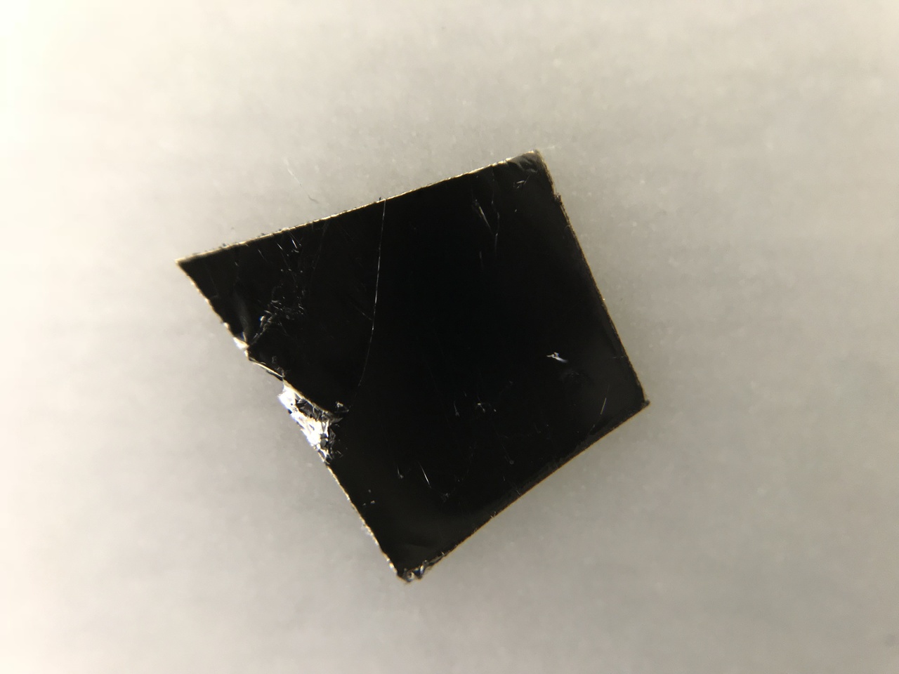
Zirconium disulfide (ZrS₂) is an indirect gap layered semiconductor in the bulk and becomes direct gap semiconductor in monolayer form. They are designed and optimized in the last three years to achieve perfect industrial semiconductor grade materials with: 1) excellent stoichiometry, 2) large single domain size, 3) single phase materials without any mixed phases or amorphous content, 4) perfect layered crystal ideal for exfoliation purposes with impressive mosaic spread 0.08 degrees, 5) unmatched purity -semiconductor grade (5.5N), 99.9995%.
Growth method matters> Flux zone or CVT growth method? Contamination of halides and point defects in layered crystals are well known cause for their reduced electronic mobility, reduced anisotropic response, poor e-h recombination, low-PL emission, and lower optical absorption. Flux zone technique is a halide free technique used for synthesizing truly semiconductor grade vdW crystals. This method distinguishes itself from chemical vapor transport (CVT) technique in the following regard: CVT is a quick (~2 weeks) growth method but exhibits poor crystalline quality and the defect concentration reaches to 1E11 to 1E12 cm-2 range. In contrast, flux method takes long (~3 months) growth time, but ensures slow crystallization for perfect atomic structuring, and impurity free crystal growth with defect concentration as low as 1E9 - 1E10 cm-2. During check out just state which type of growth process is preferred. Unless otherwise stated, 2Dsemiconductors ships Flux zone crystals as a default choice.
Characterization
Each batch of material growth products are characterized using XRD, XPS, TEM, SIMS, Raman, PL, and Optical absorption techniques to ensure crystal quality and reproducibility. XRD, Raman, and PL measurements are performed on every delivered sample. Each other is ideal for 100s of monolayer production and is sufficient for 3-9 months using exfoliation tips.
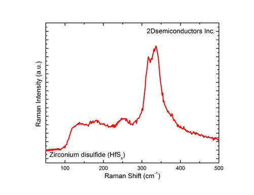
Raman spectroscopy is data is taken on every item. Typically, flakes show two prominent Raman peaks at 318 cm-1 and 335 cm-1.
Possible applications:
Electronics
Sensors - detectors
Optics
STM – AFM applications
Molecular detection – binding
Ultra-low friction studies (tribology)
Materials science and semiconductor research


7天即到
本地发货
满500元
免运费

支持信用卡在线支付
和银行转账

客服电话:400-701-7100
Email: taizhou@sunano.com.cn
 陈谷一
陈谷一