


详情
This product contains full area coverage ReSe2 monolayers on c-cut sapphire substrates. Sample size measures 1cm in size and the entire sample surface contains monolayer thick ReSe2 sheet. Synthesized full area coverage monolayer ReSe2 is highly crystalline, some regions also display significant crystalline anisotropy.
Sample Properties.
Sample size |
1cm x 1cm square shaped |
Substrate type |
Sapphire c-cut (0001) |
Coverage |
Full monolayer coverage |
Electrical properties |
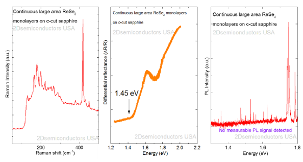
1.45 eV Anisotropic Semiconductor (Indirect Bandgap) |
Crystal structure |
Distorted Tetragonal Phase (1T’) |
Unit cell parameters |
a = 0.656 nm, b = 0.672 nm, c = 0.674 nm, α = 91.74°, β = 105°, γ = 119° |
Production method |
Atmospheric Pressure Chemical Vapor Deposition (APCVD) |
Characterization methods |
Raman, angle resolved Raman spectroscopy, photoluminescence, absorption spectroscopy TEM, EDS |
Specifications
1) Identification. Full coverage 100% monolayer ReSe2 uniformly covered across c-cut sapphire
2) Physical dimensions. One centimeter in size. Larger sizes up to 2-inch wafer-scale available upon requests.
3) Smoothness. Atomically smooth surface with roughness < 0.15 nm.
4) Uniformity. Highly uniform surface morphology. ReSe2 monolayers uniformly cover across the sample.
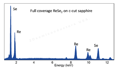
5) Purity. 99.9995% purity as determined by nano-SIMS measurements
6) Reliability. Repeatable Raman and photoluminescence response
7) Crystallinity. High crystalline quality, Raman response, and photoluminescence emission comparable to single crystalline monolayer flakes.
8) Substrate. c-cut Sapphire but our research and development team can transfer ReSe2 monolayers onto variety of substrates including PET, quartz, and SiO2/Si without significant compromisation of material quality.
Defect profile. ReSe2 monolayers do not contain intentional dopants or defects. However, our technical staff can produce defected ReSe2 using α-bombardment technique.
Supporting datasets [for 100% Full area ReSe2
monolayers on c-cut Sapphire] Transmission electron images (TEM) and angle resolved Raman spectroscopy
measurements acquired from CVD grown full area coverage ReSe2 monolayers on
c-cut sapphire confirming crystalline anisotropy Energy dispersive X-ray spectroscopy (EDX) characterization on CVD grown
full area coverage monolayer ReSe2 on c-cut sapphire Raman spectroscopy measurement confirm monolayer nature of the CVD grown
samples. Differential reflectance measurements clearly show band gap at 1.45 eV
for monolayer ReS2 consistent with the existing literature values. PL spectrum
does not show any PL signal due to indirect band nature.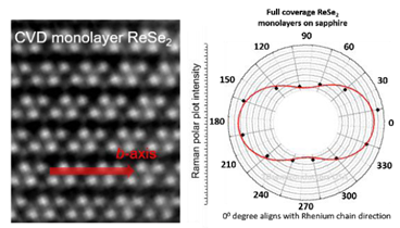


7天即到
本地发货
满500元
免运费

支持信用卡在线支付
和银行转账

客服电话:400-701-7100
Email: taizhou@sunano.com.cn
 陈谷一
陈谷一