


详情
Substrate:
Sapphire (c-cut)
Quartz (Silica)
TEM grids (please supply grids)
Thermal Oxide (SiO2/Si)
Polyethylene terephthalate – PET Substrates
Pick your own substrates (please define the substrate type)
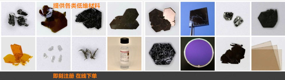
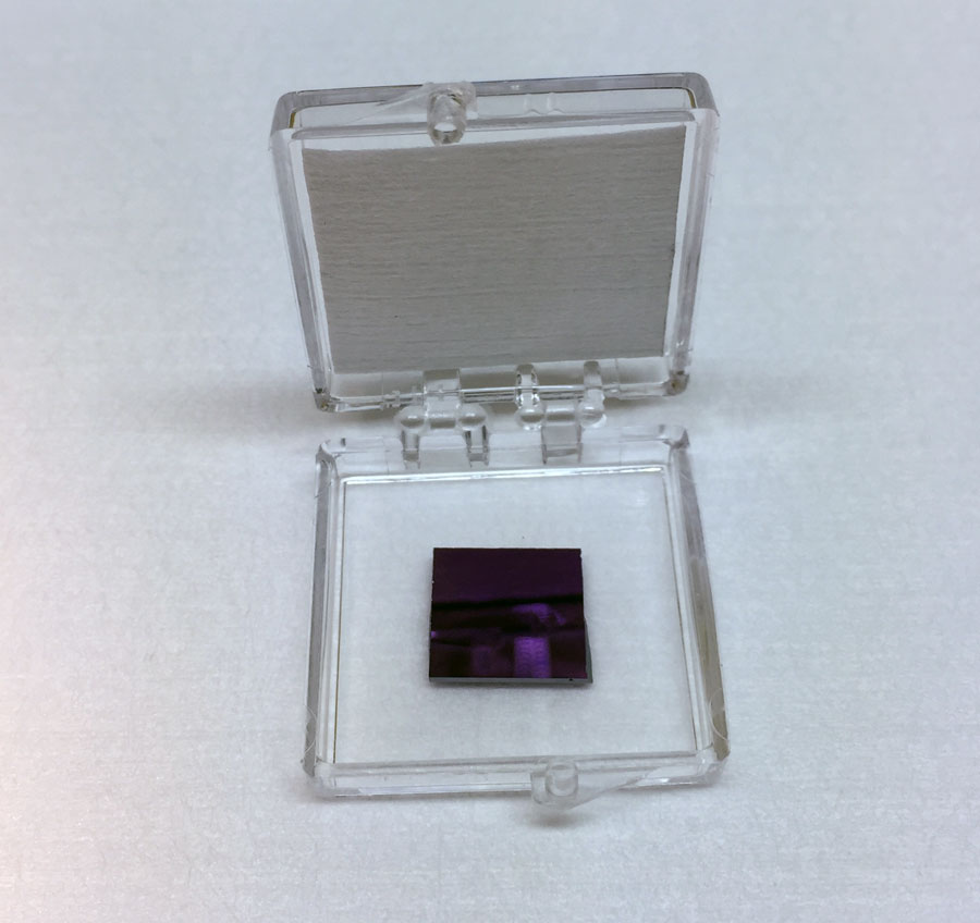
Our R&D has developed scalable methods to transfer large area h-BN, graphene, MoS2, MoSe2, WS2, WSe2, ReS2, ReSe2, SnS2, SnSe2, PtS2, and PtSe2 sheets onto almost any substrates (please see Question 3 below). Our team uses extremely delicate steps and processes to keep the 2D layers clean and unaltered. Our processes are carried out under ultra-high purity environment so that the material quality is not sacrificed. However, because of the custom nature of the production process, all transferred CVD sales are final and non-refundable.
During the online check-out or when requesting a formal quote, please indicate desired substrate, desired CVD material (see list of CVD products here), and any additional requirements / suggestions.
Frequently asked questions
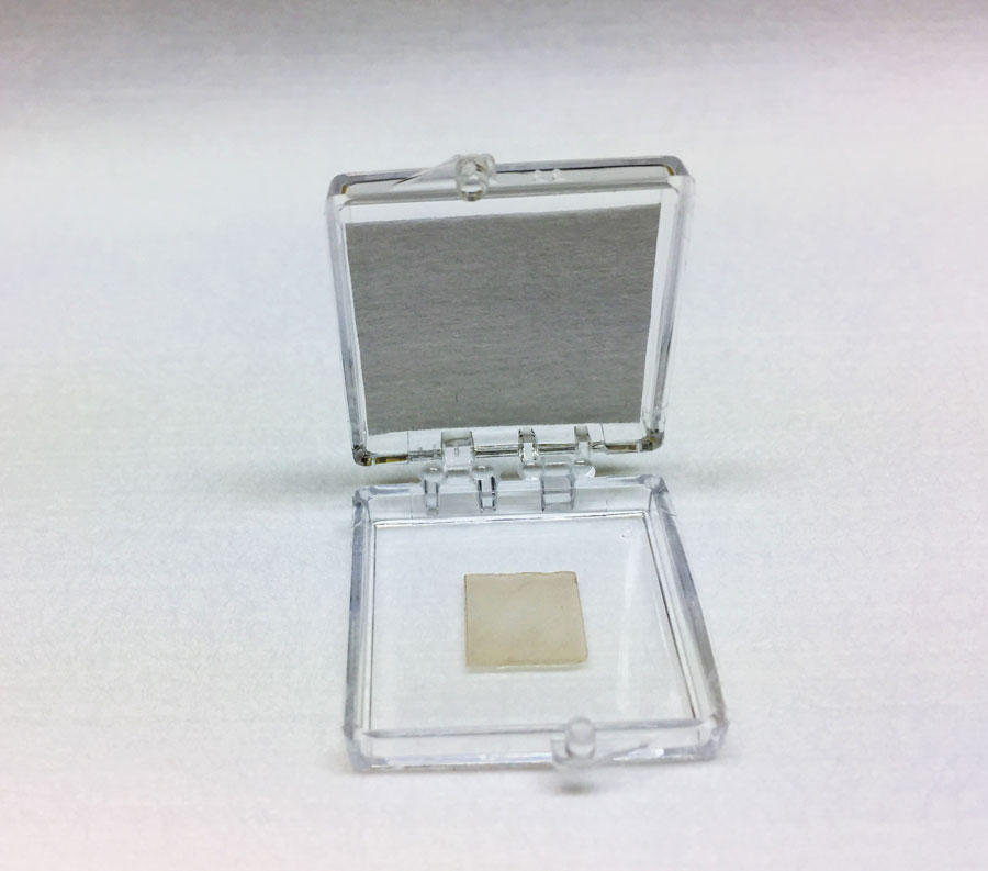
Q1: Can you transfer monolayers onto TEM grids?
A: Yes, we can transfer any CVD product onto any TEM grids. Our company requires you to select your own TEM grids, inform us the model, and send (extra) TEM grids so that we can do tests to deliver you good quality samples.
Q2: Can you guarantee that CVD monolayers will be same quality after the transfer?
A: Transfer process requires polymeric stamping and / or chemical processes. These steps generally will introduce some cracks and voids in the samples. But if you selected to transfer full area CVD monolayers, they will still be at large scales. There might be some folding, wrinkling effects, and this is normal. If your CVD monolayer is luminescent, after the transfer optical properties will remain similar with PL emission at the same wavelenghts
Q3: What kind of substrates can you transfer onto?
A: You would be surprised to know but we have transferred CVD monolayers more than 100 different substrates to date. Examples include, Bragg reflectors, plasmonic structures, SiO2/Si, sapphire, quartz, mica, PET, polymer, other 2D materials, glass, TEM grids, metals, and even on a diamond!
Q4: What is the typical processing times?
A: This will depend on your project, chemistry required, and your sets of requirements towards sample production. It is typically around 1-3 weeks.


7天即到
本地发货
满500元
免运费

支持信用卡在线支付
和银行转账

客服电话:400-701-7100
Email: taizhou@sunano.com.cn
 陈谷一
陈谷一